Hi, I’m Aleksi and I’m a Master of Science student in the field of technology, material science, at Aalto University. Actually, it was a summer job at Murata that first got me interested in material science. I was able to see how silicon, a quite simple and common material, could be cleverly processed into inconceivable structures that are then electrified. And the end result could even save a driver’s life, for example! I realized that nature is quite complex and that studying would really allow me to make the world a better place, at least for someone.
How did I get to Murata?
In 2017, pouring coffee at Helsinki Airport during my student years started to get boring, and I wanted to find a new summer job, preferably something with machines. During school courses, at my student society and when talking with my friends, I heard about a classic job opportunity for process engineering students, Murata.
May was quickly approaching, but I decided to send in my application, and was quickly invited for an interview. Nerve-wracking. However, the actual in-person interview was a relaxed event. We got to know the process and the plant, and then basically agreed that I will come back soon to sign an employment contract. Fantastic!
What did I do at Murata?
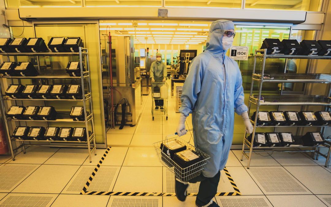
I started my work at Murata in May 2018 in a weekend shift at the smaller ADP line used at the time. There, I was able to see how the products are placed in their protective housing. The few weeks of training flew past, and the rest of the summer I spent twisting the cut wires of a wire bonder, carrying out tensile testing and, of course, cleaning the gel machine. Such meditative work.
The summer slipped past quickly, and it changed my interests and my studies from chemistry to material technology. Next summer, it was an easy decision to contact my previous boss and continue from where I started at the assembly. However, something was missing. ADP line’s Inkku the Robot, who somewhat temperamentally transported batches from one machine to the next, had retired or been put to rest. RIP. In any case, Inkku’s decades-long career was now over, and the operators transported the batches between the machines, instead. This added some challenge to the work compared to the previous summer with a guessing game of ‘do you remember where this batch was supposed to go’. The fancy blue ‘Smurf’ costumes were also replaced with green coveralls.
Still, the summer went past even quicker than before, and I became more familiar with the process and the people. As my studies progressed and became more specific, I wanted to either start working as a summer engineer or see how lithography is done at Murata. I was accepted for weekend shifts at lithography. I felt like a little boy at a candy store when I was allowed to actually use the machines and run the processes I had only read about in my courses for years.
The training was quite a challenge, but the great team finally helped me learn the use of all the litho cell machines. After this, things got busy when I was allowed to run our small FAB 3 litho. It was challenging, but also very rewarding to get to finish the day while admiring the even, green machine utilization rate beams of production control tool while waiting for the next shift to arrive.
What did I get?
My wages, knowledge, skills and discussions. I was able to complement my studies through practical experience with the help of the best possible colleagues, learn new things about the process by constantly harassing the great technicians and maintenance team on the wafer side with my questions, and get some insight about the thoughts of engineers by browsing the network drives, online Thesis folders and the Streams service. Interesting times. I am now continuing my master’s studies this autumn, and I will definitely reserve a spot for the MEMS design course by Murata and Aalto University in my schedule. I can’t wait to see what duties my future will bring. My sincerest thanks to everyone!
Aleksi Pajunen,
Processing Operator
*Lithography is a production step in which the structures contained in the sensors can be made by etching silicon.

Recent Comments