Hi, I’m Pinja and I’m a student majoring in functional materials at Aalto University. I’m starting my last year of master’s studies in the fall. As a student in material technology, I had pictured myself in a summer job where I would have the chance to get practical experience in electronic applications and solve problems related to them. Murata as a company has come up on several occasions during my studies. When browsing Murata’s website, I noticed that they produce electronics for various important applications such as cars, airplanes and even pacemakers.
My path to a Murata summer job
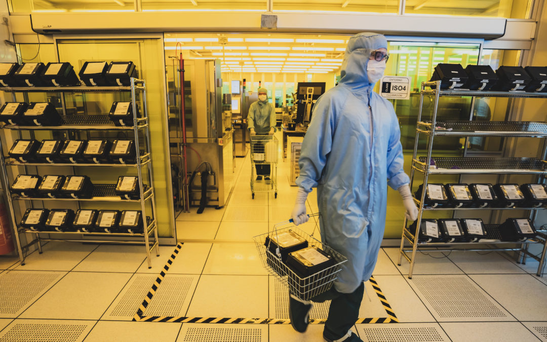
The field of semiconductor technology was already familiar to me from my previous job as a production worker in another company, so I had the courage to apply for the summer job at Murata. After the exciting application process, I was selected to work at Murata as a process development (PD) trainee in photolithography for the summer of 2021. In a nutshell, photolithography involves patterning a resist on top of a wafer by exploiting its chemical reaction with light. This summer, I continued my job as a PD trainee in photolithography and I have also started writing my thesis.
Work experience provided by Murata
I spent my first summer learning new processes and, after my initial orientation, I was able to get into my actual work duties as a PD trainee in photolithography. During the first summer, I already got to take responsibility in my own projects, and I got through any difficulties with the help of my team. In this job, you usually get to use your own imagination, but sometimes mistakes happen to all of us. However, you should trust yourself and not feel too guilty about failing, because you can only succeed at things if you try.
Murata proposed a subject for my thesis, which I then accepted. At a general level, my thesis explores the production of three-dimensional shapes in photolithography. This research topic has potential in several areas, such as time and material savings. Usually, when people think of environmental efforts, they only think about how we could recycle more efficiently. In PD, you can design processes to be more efficient in a new way. Photolithography takes a big chunk out of the processing time of electronics, so even a small change in the use of materials can make a big difference. Electronics are also needed in so many applications, which means that a slightly more efficient process may decrease consumption significantly.
During my time at Murata, I have learned in particular how long the MEMS sensor manufacturing process is and how it could be improved, specifically in terms of photolithography. I also have more confidence in my own judgement now that I have been able to work independently in the production facilities and freely make my own suggestions for improvement.
Observations about working at Murata
One of the most interesting things I have noticed during my time at Murata is that there is only one designated expert for many of the processes and devices. As an expert, you get to focus intensively on a specific subject and develop it to be more effective. As a student, I also appreciate that you can easily combine your studies with work. Murata also takes safety and working methods seriously, which is particularly important when working in electronics manufacturing.
Future career plans
In the future, I see myself in a work environment where I can use my strengths such as my problem-solving skills and my fearless approach to new challenges. I could see myself working at Murata after graduation, since Murata offers great career advancement opportunities and there is always work here to be done.

Recent Comments